Kodera Laboratory
Research
We develop semiconductor quantum devices and the technologies needed to fabricate, control, read out and integrate them.
Scalable spin-qubit readout
Spin-to-charge conversion makes a spin state accessible to electrical measurement. We study low-noise cryogenic amplification and charge sensing, with attention to bandwidth, power dissipation, wiring and the space available inside a refrigerator. Our aim is to develop readout systems that can be extended to larger numbers of qubits.
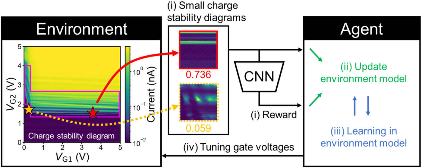
Automated tuning with machine learning
Each quantum-dot device requires careful adjustment of gate voltages. We investigate machine-learning methods, including model-based reinforcement learning, to automate this process. Our work includes constructing environment models from silicon quantum-dot measurement data and developing methods that can be extended to more complex devices.
Radio-frequency reflectometry
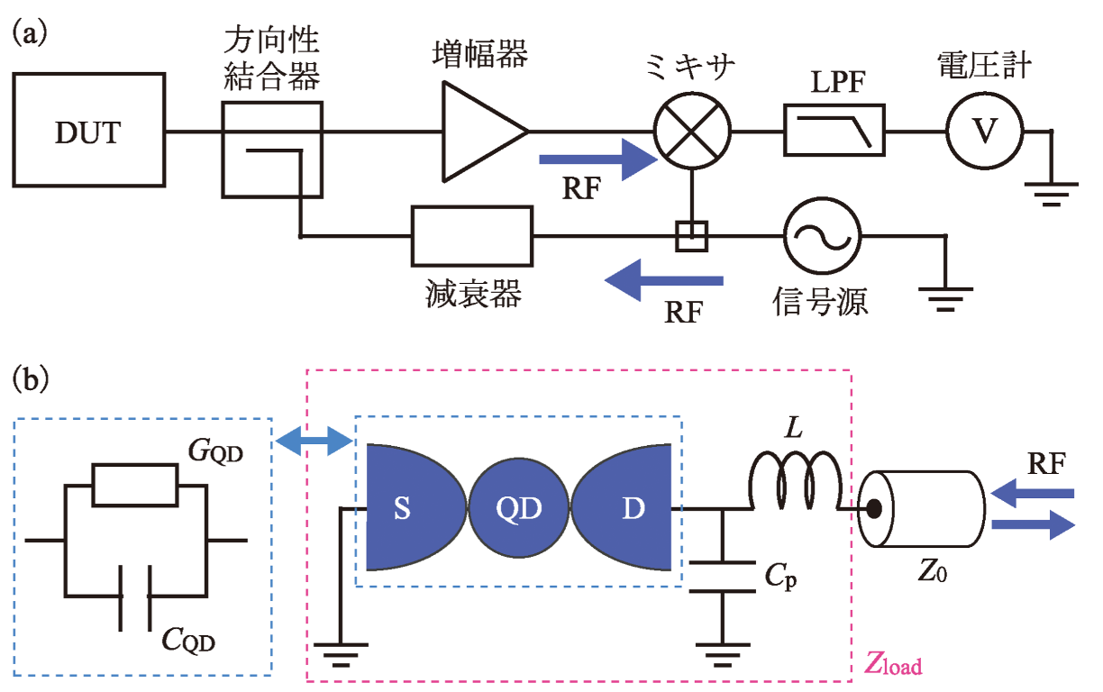
RF reflectometry measures changes in a device’s electrical response through a matching circuit. We study tunable impedance matching at cryogenic temperatures, mixed-mode transmission to reduce crosstalk, and matching circuits for frequency multiplexing. Current work also covers IQ-encoded readout, parametric amplification and cryogenic oscillators.
Hole-spin control in silicon
We investigate hole spins in physically defined p-type silicon quantum dots fabricated by etching silicon-on-insulator substrates. Spin–orbit coupling offers a route to electrical spin control without additional magnetic structures. We study device designs and operating conditions that support integration and operation at higher temperatures.
Triangular triple quantum dots
Three quantum dots arranged in a triangle provide a small building block for two-dimensional integration. We fabricate silicon devices and develop charge sensing, pulsed measurements and RF single-electron-transistor techniques toward fast spin readout. These measurements give access to individual tunnelling events and the dynamics of confined carriers.
Long-range interactions
Coupling distant qubits is a challenge as quantum processors grow. We investigate interactions between the outer dots of serial triple quantum-dot devices in silicon, exploring routes beyond interactions between nearest neighbours.
Device structures for integration
Physically defined silicon quantum dots can reduce the number of gates needed to form a device. We model electrostatic potentials and carrier distributions in silicon-on-insulator structures to guide device geometry, fabrication and measurement.
Two-dimensional qubit architectures
We study arrangements of Si/SiGe quantum dots for larger quantum processors, including architectures for noisy intermediate-scale quantum systems. This work is carried out with collaborators at RIKEN and considers how the small footprint of semiconductor spin qubits can support two-dimensional integration.
Cryogenic CMOS and quantum-device integration
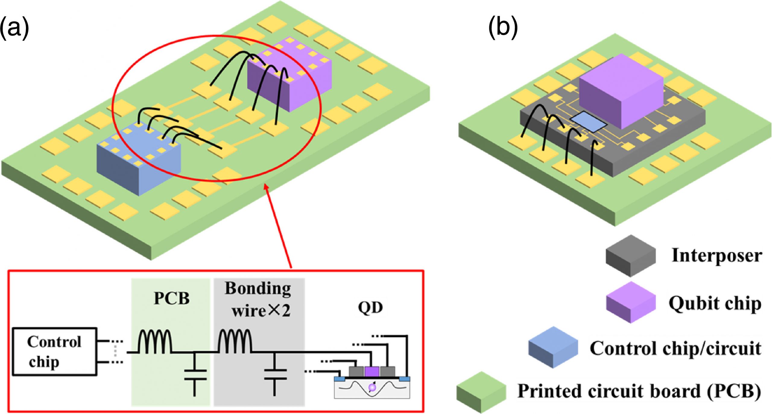
Room-temperature control electronics and their wiring place thermal and spatial demands on cryogenic systems. In collaboration with the Nagata–Miki laboratory at Kobe University, we study the integration of silicon quantum-dot devices with cryogenic CMOS circuits. Our work includes flip-chip connections to active interposers with electrostatic-discharge protection and selector circuits.
Germanium quantum dots
Germanium hole systems combine a small effective mass with strong spin–orbit coupling. We fabricate and characterize germanium quantum dots, aiming to improve device performance and develop structures suitable for integrating hole-spin qubits.
Single-electron transport with acoustic waves
Surface acoustic waves can provide a way to move individual electrons between separated quantum dots. We aim to develop this approach in silicon, exploring a potential connection between local quantum devices and more distributed quantum-information architectures.
Noise spectroscopy and correlations
Understanding noise is essential for improving qubit control and device design. We analyze noise spectra in individual silicon quantum dots, correlations between dots, and fluctuations associated with interdot tunnelling. These measurements help distinguish sources of noise and guide the design of integrated devices.
Silicon qubits at elevated temperatures
We aim to operate silicon spin qubits at approximately 1–2 K, above the temperatures commonly used in spin-qubit experiments. Higher operating temperatures could allow more cooling power for nearby electronics. We investigate spin dynamics, operating points that preserve quantum information, and the relative advantages of electron and hole systems.
Related publications
Find the original papers, authors and publication details in our publication list. The Japanese research page includes additional experimental figures and references.